Author Affiliations
Abstract
National Institute of LED on Silicon Substrate, Nanchang University, Nanchang 330096, China
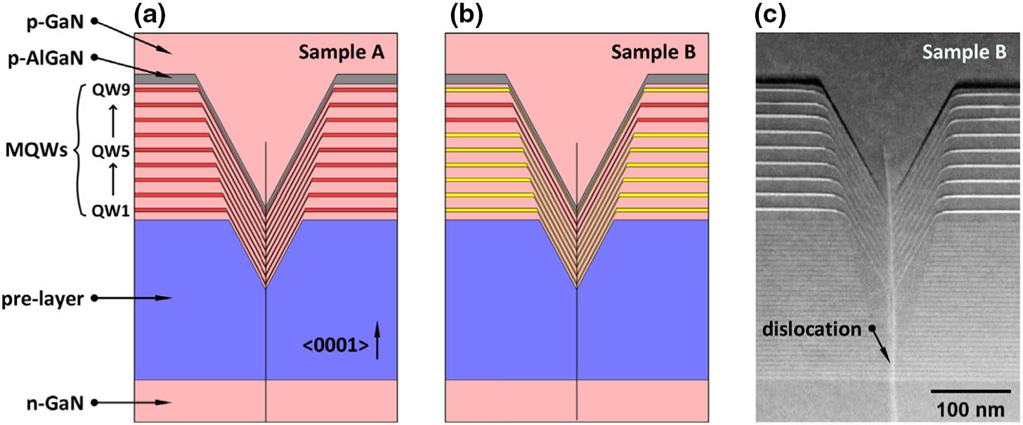
Indium gallium nitride (InGaN)-based light-emitting diodes (LEDs) are considered a promising candidate for red-green-blue (RGB) micro displays. Currently, the blue and green LEDs are efficient, while the red ones are inefficient for such applications. This paper reports our work of creating efficient InGaN-based orange and red LEDs on silicon(111) substrates at low current density. Based on the structure of InGaN yellow LEDs, by simply reducing the growth temperature of all the yellow quantum wells (QWs), we obtained 599 nm orange LEDs with peak wall-plug efficiency (WPE) of 18.1% at . An optimized QW structure was proposed that changed two of the nine yellow QWs to orange ones. Compared with the sample containing nine orange QWs, the sample with two orange QWs and seven yellow QWs showed similar emission spectra but a much higher peak WPE up to 24.0% at with a wavelength of 608 nm. The improvement of peak WPE can be attributed to the improved QW quality and the reduced active recombination volume. Subsequently, a series of efficient InGaN-based orange and red LEDs was demonstrated. With further development, the InGaN-based red LEDs are believed to be attainable and can be used in micro LED displays.
Photonics Research
2020, 8(11): 11001671
Author Affiliations
Abstract
National Institute of LED on Silicon Substrate, Nanchang University, Nanchang 330096, China
The impact of the V-pits covering layer (VCL) position on the optoelectronic performance of InGaN-based green light-emitting diodes (LEDs) was investigated. It is found that earlier covering of V-pits will hinder the hole injection via the sidewall of V-pits, and then result in less quantum wells (QWs) participating in radioluminescence. The current-voltage characteristics show that the LEDs with earlier covering of V-pits have higher operating voltage at room temperature, and a more dramatic voltage rise with the reduction of temperature. Meanwhile, more manifested emission peaks for sidewall QWs and deeper QWs near to n-type layer was observed in the sample with earlier coveing of V-pits at cryogenic temperatures, for the reason that the holes being injected via V-pits sidewall have higher kinetic energy and could transport to deeper QWs.
Journal of Semiconductors
2019, 40(5): 052801
Author Affiliations
Abstract
1 National Institute of LED on Silicon Substrate, Nanchang University, Nanchang 330096, China
2 Nanchang Yellow Green Lighting Company Limited, Nanchang 330096, China
3 e-mail: liujunlin@ncu.edu.cn
Realization of efficient yellow-light-emitting diodes (LEDs) has always been a challenge in solid-state lighting. Great effort has been made, but only slight advancements have occurred in the past few decades. After comprehensive work on InGaN-based yellow LEDs on Si substrate, we successfully made a breakthrough and pushed the wall-plug efficiency of 565-nm-yellow LEDs to 24.3% at 20 A/cm2 and 33.7% at 3 A/cm2. The success of yellow LEDs can be credited to the improved material quality and reduced compressive strain of InGaN quantum wells by a prestrained layer and substrate, as well as enhanced hole injection by a 3D pn junction with V-pits.
Photonics Research
2019, 7(2): 02000144
1 中国科学院半导体研究所, 北京半导体照明科技促进中心, 北京 100083
2 南昌大学 国家硅基LED工程技术研究中心, 南昌 330047
采用条形Al掩模在Si(111)衬底上进行了GaN薄膜侧向外延的研究。结果显示, 当掩模条垂直于Si衬底[11-2]方向, 也即GaN[10-10]方向时, GaN无法通过侧向生长合并得到表面平整的薄膜; 当掩模条平行于Si衬底[11-2]方向, 也即GaN [10-10]方向时, GaN侧向外延速度较快, 有利于合并得到平整的薄膜。同时, 研究表明, 升高温度和降低生长气压都有利于侧向生长。通过优化生长工艺, 在条形Al掩模Si(111)衬底上得到了连续完整的GaN薄膜。原子力显微镜测试显示, 窗口区域生长的GaN 薄膜位错密度约为1×10⁹/cm2, 而侧向生长的GaN薄膜位错密度降低到了5×10⁷/cm2以下。
侧向外延过生长 氮化镓 硅 ELOG GaN Si MOCVD MOCVD


